Being a printed circuit board designer can be very rewarding and some find it incredibly relaxing, but how do you actually become one? Let’s break it down a little, starting from the very top and beginning with ‘where did it all begin?’.
Paul Eisler, an Austrian inventor, is widely accredited with the invention of the printed circuit board whilst he was working on a radio in England around 1936. In the early 1940s, the USA began using this new technology to create proximity fuses which would detonate automatically based on a pre-determined distance. The PCB didn’t become popular, however, until the 1950s and since then, every single decade has seen a new invention that makes the field of PCB design exciting and innovating.
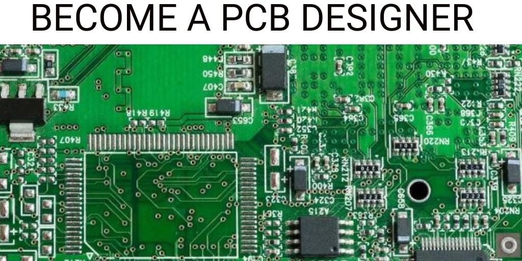
The relentless march of technology, in general, has seen hand-made printed circuit boards evolve into complex, multi-layered boards.
Why Do We Need Printed Circuit Board Designers?
Printed circuit boards are the foundation technology of any electronic device, regardless of what it might be. Expanding horizons in the field of electronics has seen tremendous demand for trained, experienced printed circuit board designers. There are plenty of job opportunities just waiting for the right PCB designer. The consumer, and industry, demand new and improved electronic devices all the time so this area of technology is what is known as ‘evergreen’.
A printed circuit board designer creates models, or footprints, for the components that will be included on the PCB using circuit board design software, such as Altium Designer.The designer will then create the board design within that software using the information from the footprints they have created.
Trace Routing
When all of the footprints required have been created and placed upon the board, the designer will then add all of the components using lines in a process called trace routing. The used software can do this automatically but for more complex designs, the designer may choose to do this manually to ensure everything is connected as it should be.
Educational Requirements For PCB Design Engineers
Many companies require that designers have a degree in electronics. If you have a strong desire for learning and to explore and you have or are willing to attain a bachelor’s degree, diploma or masters in electronics then this could well be the career for you.
Sadly, there are no specific degrees for this kind of design. PCB design tool companies do provide training for specific tools however, but the above mentioned degrees are currently the best option.
Hands on experience is also a great way to show your level of competence and so designing something at home on your own time is an excellent way to showcase your talent, and your passion for printed circuit board design.
You may also find that there are companies that do require any formal degrees at all, perhaps in recognition of the fact there are no specific qualifications that can be attained beyond hands on experience. That being said, being able to demonstrate a working knowledge of CAD software will still go a long way.
")


")